LM2917 Frequency to Voltage Converter Circuit Diagram An on-chip zener clamp produces a regulated and stabilized frequency to voltage or current conversion (only in LM2917s) A typical connection diagram of the IC LM2907/LM2917 is shown below: Using IC LM331. Another simple frequency to voltage converter can be seen in the above circuit diagram, using a single IC LM331.

Here Frequency to Voltage Converter Circuit using 555 Timer designed to implement in such projects and applications. Simple Sensor Gauge using ESP32 Web Server. March 15, 2025. Team Digital. ESP32 Projects. Control ESP32 GPIO Pins using Web Bluetooth. March 9, 2025.

FREQUENCY TO VOLTAGE CONVERTER CIRCUIT diagram
Here is a very simple circuit diagram of a frequency to voltage (F to V) converter. Such a circuit finds numerous applications in projects like digital frequency meters, tachometers etc. The circuit is mainly based on a LM555 timer IC. The IC is wired in mono shot mode to convert the input frequency into a fixed pulse width, variable frequency

IC LM331 Family of Voltage to Frequency and Frequency to Voltage converters are ideally suited for use in simple low cost circuits and applications like, analog to digital conversion, precision frequency to voltage conversion, linear frequency modulation or demodulation, and many other functions. At its core, a frequency to voltage converter circuit diagram is relatively simple, and consists of three basic components: an oscillator, an amplifier, and a rectifier. The oscillator is responsible for generating the high frequency signal that will be converted. The project goal is to design an embedded system (hardware/firmware) that takes in a frequency input signal. Maybe from a motor encoder or whatever and measure the frequency then convert it to analog voltage signal at the output. Of course, F/V converter integrated circuits (ICs) and other solutions are viable options indeed.
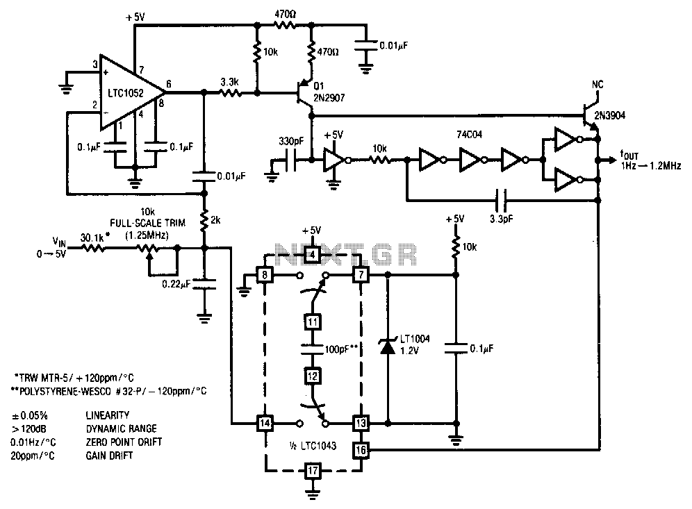
Frequency To Voltage Converter Circuit Diagram
Theory of Operation Qualitative Description. The circuit operation is fairly straightforward. When the input signal goes low, C 1 charges through D 1.It is critical that C 1 charge quickly relative to the period. This circuit depends on the transfer a fixed quantity of charge at the same rate as the input signal. in a very simple linear relationship. In our application Vcc = 5V and we wish to see a maximum output voltage of 5V as well, therefore we are given a simple design equation relating our component values to the maximum expected frequency of our input signal. (3) Choosing a value for is relatively trivial. For low frequency signal acquisition the
